Advanced PCB design service
Our PCB design service specializes in delivering comprehensive solutions, from concept to production. We offer design, prototyping, testing, and validation of both analog and digital systems, with a focus on high-performance and complex circuits.
Our end-to-end PCB design service is ideal for clients needing reliable, innovative solutions across various industries, including telecommunications, automotive, aerospace, consumer electronics, and industrial automation.
By combining state-of-the-art tools, engineering expertise, and a commitment to quality and efficiency, we ensure your project is delivered on time, within budget, and optimized for performance and longevity.
Key Capabilities:
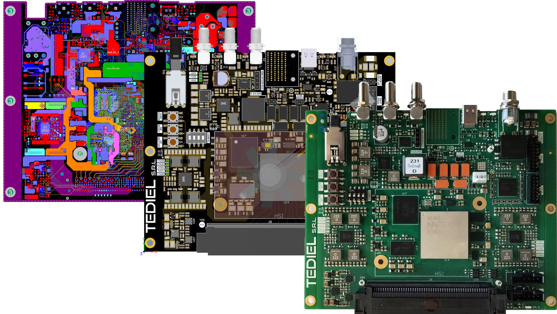
High-Speed Digital PCB Design We excel in the design of high-speed digital PCBs that accommodate cutting-edge technologies such as FPGAs, DDR, and QDR memories, and System-on-Chip (SoC) solutions. Our designs ensure signal integrity, power distribution optimization, and reliability under demanding conditions. We integrate peripherals like networking interfaces, video controllers, and communication modules to meet the specific needs of your application.
Advanced Analog Circuit Design Our team can handle intricate analog PCB designs with stringent noise control, precision timing, and high-resolution data acquisition requirements.
Low-Power and IoT Solutions We develop circuits tailored for low-power applications, e.g. for IoT devices, that utilize the latest ARM-based microprocessors and energy-efficient architectures. We cover for battery life optimization, wireless communication, and sensor integration, ensuring that your IoT solution is robust, scalable, and future-ready.
Prototyping & Testing We offer a rapid prototyping service to help bring your designs to life quickly.
Design for Manufacturability (DFM) & Assembly (DFA) Our team considers manufacturability and assembly at every step of the design process, ensuring that the transition from design to production is seamless. We collaborate closely with manufacturers to optimize yield, cost, and time-to-market